Learn it by examples – (Timers)
By David Kebo Houngninou
On this page, you will find some interfacing experiments using the ARM Cortex M3.
– The evaluation board we target is the MCBSTM32C running on the STM32F107VC microcontroller.
– The tutorial focuses on configuring the MCBSTM32C and interfacing.
– Datasheets and documentation for STMicroelectronics STM32F107VC core is available at: http://www.keil.com/dd/chip/4889.htm.
– The reference used for this tutorial is the RM0008 Reference manual for STM32F107xx advanced ARM®-based 32-bit MCUs.
Tutorial 4: Timers
Timers are clock sources used as the ‘heartbeats’ for operations.
e.g. of applications using timers:
- Counting pulses
- Measuring time periods of waveforms
- Generating pulse width modulation (PWM) signals
- Triggering external devices
- Timing special events
03 groups of timers:
- Basic Timers
- General Purpose Timers
- Advanced Timers (TIM1&TIM8)
1- Basic Timers
TIM6, TIM7
Applications:
no I/O channels for input capture
no PWM generation
Only used for time-base generation
2- General Purpose Timers
TIM2, TIM3, TIM4, TIM5
Applications:
PWM generation
Input capture
Time-base generation
Output compare
3- Advanced Timers
TIM1, TIM8
Applications:
Advanced PWM generation
Input capture
Time-base generation
Output compare
Timers pin
Each timer is associated with an I/O pin
Configure the alternate function to use the timer pin
What is an alternate function (A.F)?
In addition to general-purpose input and output the ARM subsystem can implement other specialized input output functions.
e.g. TIM4_Ch4 is an alternate function for pin PB9
TIMx functional description
The main block of the timer is a 16-bit counter TIMx_CNT with an auto-reload register TIMx_ARR
The counter can count up, down, or both up and down.
The counter clock can be divided by a pre-scaler TIMx_PSC
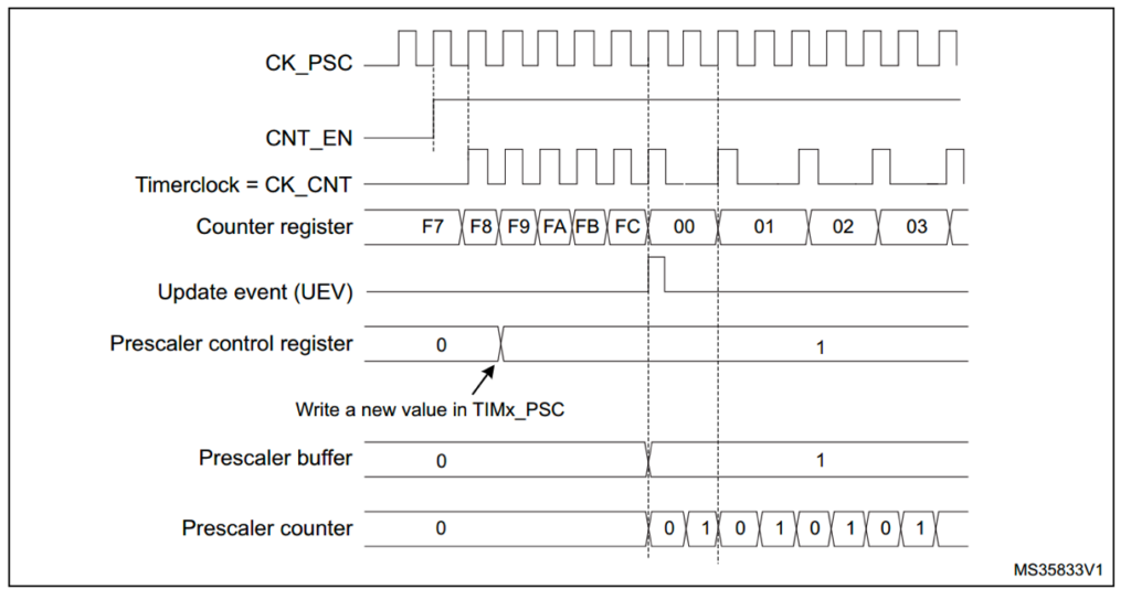
TIMx functional description
Counter timing diagram with pre-scaler division change from 1 to 2
Timer configuration
RCC->APB1ENR //Enable clock to the timer
RCC->APB2ENR //Enable the Alternate function and the GPIO clock
(TIMx_SMCR)TIMx slave mode control register //Set the internal clock as system clock
(TIMx_PSC)TIMx pre-scaler register // Set the pre-scaler
(TIMx_CR1)TIMx control register // Enable the timer
Steps:1.Enable clock to the timer |
Notes about the clock usage:The HSI clock signal is generated from an internal 8 MHz RC oscillator and can be used directly as a system clock. To set the pre-scaler register: |
|---|
Timer example
A developer is writing a function for a counter user a timer.
The internal HIS clock signal runs at 8 MHz
What is the value to set the pre-scaler to count every millisecond?
1 2 3 4 |
CK_CNT = fCK_PSC / (PSC[15:0] + 1) PSC[15:0] + 1 = fCK_PSC / 1000 PSC[15:0] = (fCK_PSC / 1000) - 1 PSC[15:0] = 7999 |
Timer clock
Timer clock
Advanced Peripheral Bus 1 Enable Register
1 |
RCC->APB1ENR |= (1<<2); //enable clock to TIM4. |
Timer clock
Advanced Peripheral Bus 2 Enable Register
1 2 |
// e.g: To use TIM4 RCC->APB2ENR |= (1)|(1<<3); //Enable the A.F clock and the GPIO clock |
Timer pre-scaler register
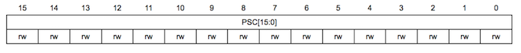
Timer pre-scaler register
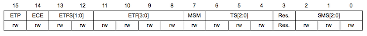
TIM1&TIM8 pre-scaler (TIMx_PSC)
PSC[15:0]: Pre-scaler value
Timer slave mode register
Timer slave mode register
TIM1&TIM8 slave mode control register (TIMx_SMCR)
SMS = 000, the pre-scaler is clocked directly by the internal clock.
Timer control register
Timer control register
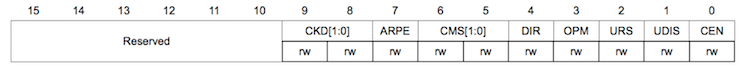
TIM1&TIM8 control register 1 (TIMx_CR1)
CEN: Counter enable
0: Counter disabled
1: Counter enabled