Learn it by examples – (ADC)
By David Kebo Houngninou
On this page, you will find some interfacing experiments using the ARM Cortex M3.
– The evaluation board we target is the MCBSTM32C running on the STM32F107VC microcontroller.
– The tutorial focuses on configuring the MCBSTM32C and interfacing.
– Datasheets and documentation for STMicroelectronics STM32F107VC core is available at: http://www.keil.com/dd/chip/4889.htm.
– The reference used for this tutorial is the RM0008 Reference manual for STM32F107xx advanced ARM®-based 32-bit MCUs.
Tutorial 2: Setup and initialize the ADC
The Analog to Digital Converter (ADC) converts an analog input to a digital input for use by the microprocessor and the Digital to Analog (DAC) takes the microprocessor’s digital output and converts it to an analog signal.
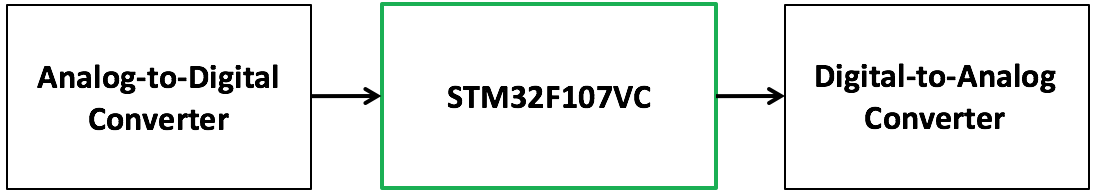
ADC to STM32F107VC to DAC
We already enabled the APB2 clock in part 1 now let’s enable the clock for the ADC.
RCC->APB2ENR |= 1 << 9; /* Enable ADC1 clock */
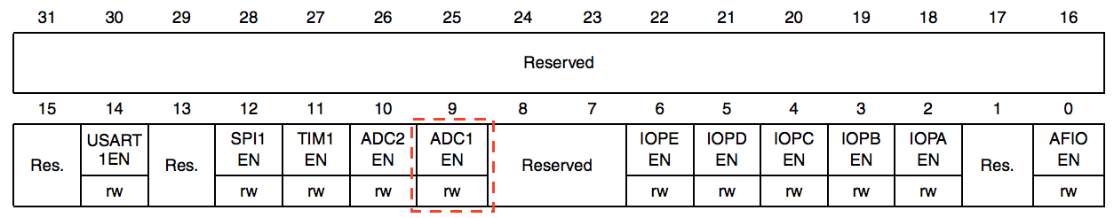
APB2 peripheral clock enable register (RCC_APB2ENR)
GPIOC->CRL &= 0xFFF0FFFF; /* Configure PC4 as ADC.14 input */
The potentiometer on the MCBSTM32C board connects to port pin PC4 (ADC12_IN14).
To use the potentiometer, pins must be configured as an analog input. By reading again Table 3 on the port bit configuration, you see that CNF4 and MODE4 must all be set to 0.
The line of code above is the same as:
GPIOC->CRL = GPIOC->CRL & 0xFFF0FFFF;
So to configure PC4 we use the following mask:
1111 1111 1111 0000 1111 1111 1111 1111
The bitwise AND of the GPIOC->CRL register content with the mask above will clear bits CNF4 and MODE4.
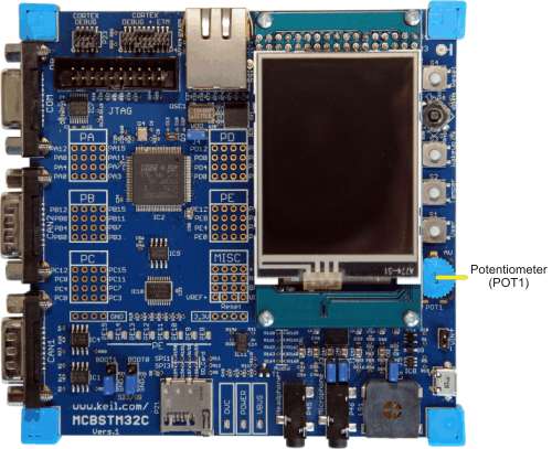
The potentiometer
ADC Sequence registers
The STM32F107 has 18 analog input channels. Sequence registers configure the number of channels to sample.
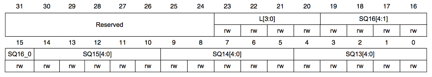
ADC Sequence registers
Bits 23:20 L[3:0]: Regular channel sequence length. Number of conversions in the regular channel conversion sequence.
0000: 1 conversion, 0001: 2 conversions, … 1111: 16 conversions
Bits 19:15 SQ16[4:0]: 16th conversion in regular sequence. The channel number is assigned as the 16th in the conversion sequence.
Bits 14:10 SQ15[4:0]: 15th conversion in regular sequence
ADC sample time registers ADC_SMPR
The potentiometer is wired to channel 14
For a single conversion:
1 2 3 |
ADC1->SQR1 = 0x00000000; // Regular channel single conversion ADC1->SQR2 = 0x00000000; // Clear register ADC1->SQR3 = (14<<0); // channel 14 as 1st conversion |
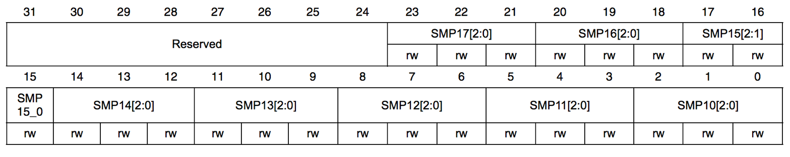
ADC sample time registers ADC_SMPR
Bits 23:0 SMPx[2:0]: Channel x Sample time selection
Select the sample time individually for each channel.
| 000: 1.5 cycles | 001: 7.5 cycles | 010: 13.5 cycles | 011: 28.5 cycles |
|---|---|---|---|
| 100: 41.5 cycles | 101: 55.5 cycles | 110: 71.5 cycles | 111: 239.5 cycles |
Table 3: ADC sample time configuration
Example
The ADC should delay reading for 5.15 uS
For an ADCCLK running at 14 MHz
Determine the sample time (Setting for SMPx)?
Answer: 5.15uS = 72 cycles at 14 MHz.
ADC Control Registers (ADC_CR)
The ADC is controlled using two control registers ADC_CR1 and ADC_CR2
Bit 8 SCAN (Scan mode): In this mode, the inputs selected through ADC_SQRx registers are converted.
Bit 5 EOCIE (Interrupt enable for EOC): enable/disable the End of Conversion interrupt.
reference: ADC block diagram (page 216) RM0008 Reference manual
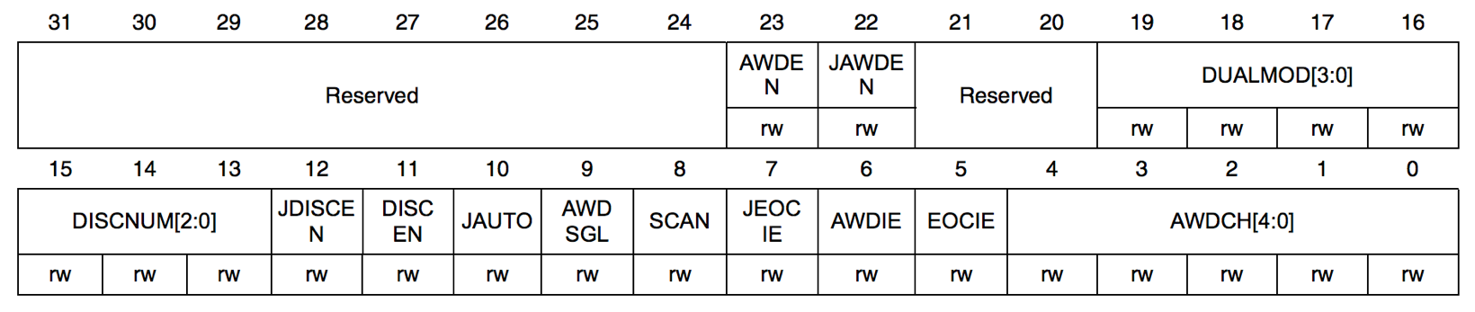
ADC Control Registers (ADC_CR)
To interrupt the microcontroller at the end of conversion:
1 2 |
ADC1->CR1 |= (1<<5); // EOC interrupt NIVC->ISER[0] |= (1<<18); //Interrupt number 18 |
ADC Control Registers configuration
1 2 3 4 5 |
ADC1->CR2 |= (7<<17); // Set SWSTART as trigger ADC1->CR2 |= (1<<20); // Enable external trigger ADC1->CR2 &= ~(1<<11); // Right data alignment ADC1->CR2 |= (1<<1); // Continuous conversion ADC1->CR2 |= (1<<0); // Turn ADC ON |
To perform all the operations above in one statement, we can use a bitwise-OR operation
Enable external trigger, EXTSEL = SWSTART, Continuous conversion, ADC enable
1 |
ADC1->CR2 = (1 << 20) | (7 << 17) | (1 << 1) | (1 << 0) ; |
ADC calibration and conversion
1 2 3 4 5 6 7 8 9 |
//Calibration ADC1->CR2 |= (1<<3); // reset calibration while (ADC1->CR2 & (1<<3)); // wait until reset finished ADC1->CR2 |= (1<<2); // start calibration while (ADC1->CR2 & (1<<2)); // wait until calibration finished //Conversion ADC1->CR2 |= (1<<22); // start SW conversion |
ADC Status and Data Registers (ADC_SR)
Bit 4 STRT: Regular channel Start flag
Bit 3 JSTRT: Injected channel Start flag
Bit 2 JEOC: Injected channel end of conversion
Bit 1 EOC: End of conversion
Bit 0 AWD: Analog watchdog flag
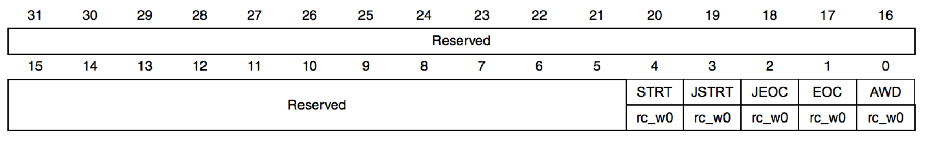
ADC Status and Data Registers (ADC_SR)
Bits 31:16, ADC2DATA[15:0]: Contains the regular data of ADC2.
Bits 15:0, DATA[15:0]: Contain the conversion result from the regular channels.
1 2 3 4 |
if (ADC1->SR & (1 << 1)) { // If conversion has finished (Check EOC bit) AD_val = ADC1->DR & 0x0FFF; // Read AD converted value ADC1->CR2 |= 1 << 22; // Start new conversion } |
Tutorial 3: Blinking the LEDs
This tutorial will explain how to blink the LEDs after they have been configured
Other project files
The following source files are required for the project.
- STM32F10x.c contains the CPU startup code for the STMicroelectronics STM32F10x devices.
- IRQ.c contains the target-dependent interrupt functions for the Timer and A/D converter.
- Retarget.c configures the target-dependent low-level functions for character I/O.
- Setup.c and Blinky.c contain the application modules that monitor analog input, provide the text output, and toggle the LEDs.
- STM32F10xR.LIB, contains the ST Software Library functions.
- LCD_4bit.c, contains the functions to produce text for the LCD display.
- Serial.c, contains the functions to communicate to the serial port.